To systematically integrate manufacturing feasibility and assembly efficiency considerations into the initial product design stage,
To achieve the goal of "designing correctly at one time and efficiently implementing production" by optimizing design schemes.
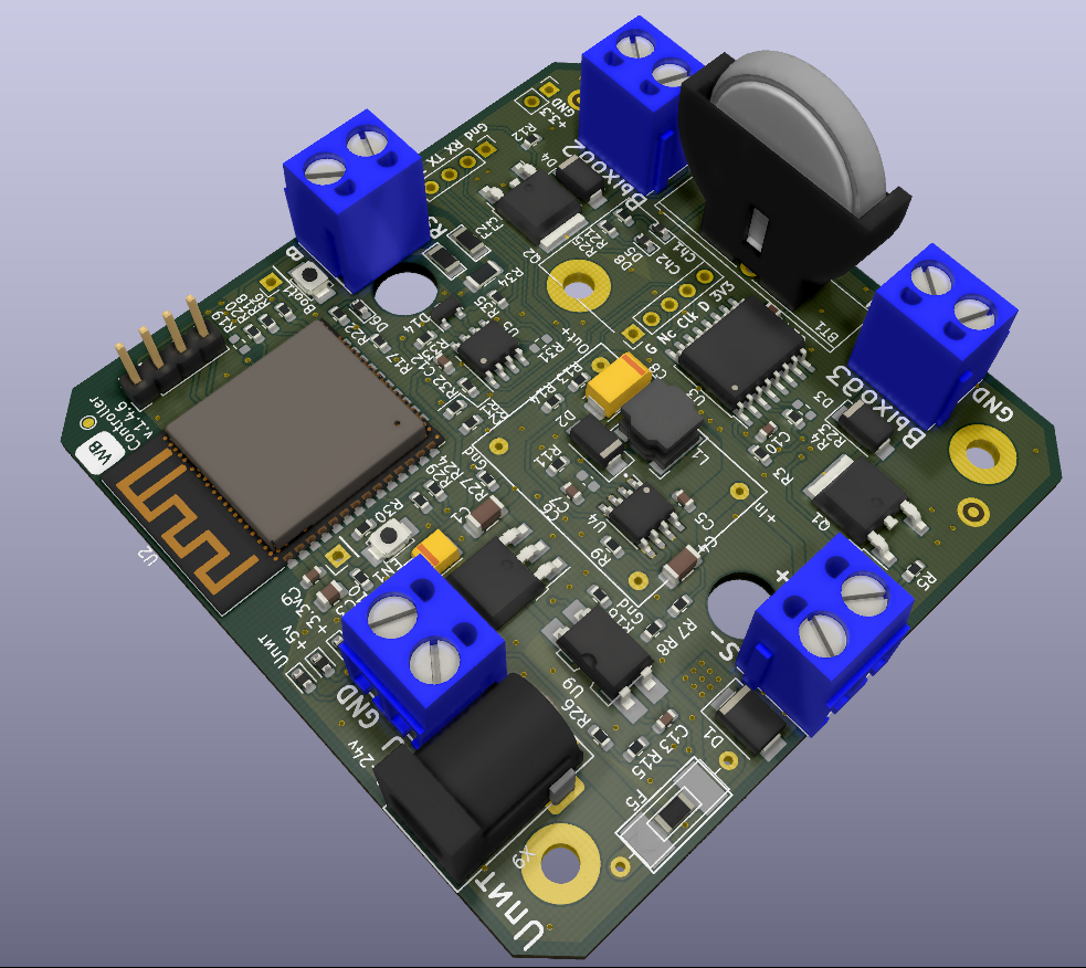
DFMA (Design for Manufacturing and Assembly) is a core proactive design methodology in the PCBA industry.It includes two core modules: DFM (Design for Manufacturing) focuses on the processability of individual PCBA components, optimizing PCB design, component selection and process adaptation; DFA (Design for Assembly) focuses on the assembly rationality of multiple components, simplifying assembly processes, reducing operation steps and error risks.


Form a cross-departmental team of Design& Manufacturing& Assembly& Quality& Procurement, clarify product functions, performance indicators, mass production scale and cost goals; formulate DFMA design guidelines and Checklist (including component selection standards, PCB design specifications, assembly process requirements); initially evaluate the feasibility of core processes and avoid high-difficulty and high-cost design schemes.


Based on Gerber files and BOM lists, conduct multi-dimensional analysis
DFM analysis
DFA analysis
Simulation verification


Produce small-batch prototypes and conduct trial production verification: check PCB manufacturing yield, component placement accuracy, and soldering quality (SPI/AOI/X-Ray inspection); verify assembly efficiency and convenience, and record assembly difficulties; optimize design based on test data and improve DFMA guidelines.


Track mass production data (yield, cost, rework rate) to identify design optimization space; conduct secondary DFMA optimization for problems exposed in mass production (such as low assembly efficiency of a certain component, high soldering defect rate in a certain area); update DFMA knowledge base and Checklist for subsequent project reuse.
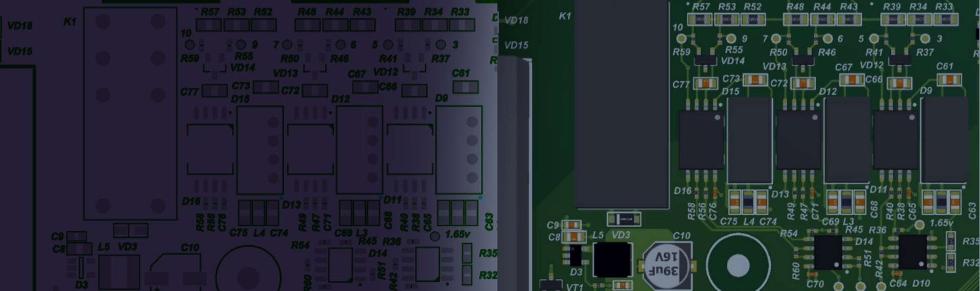
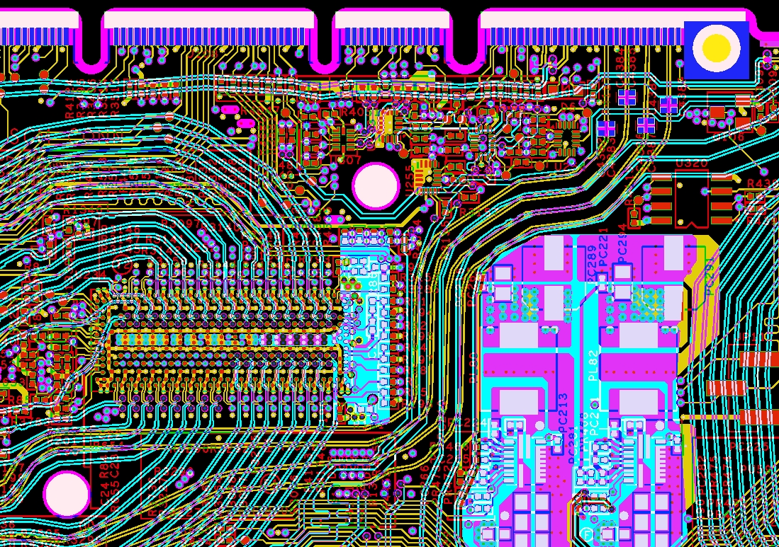
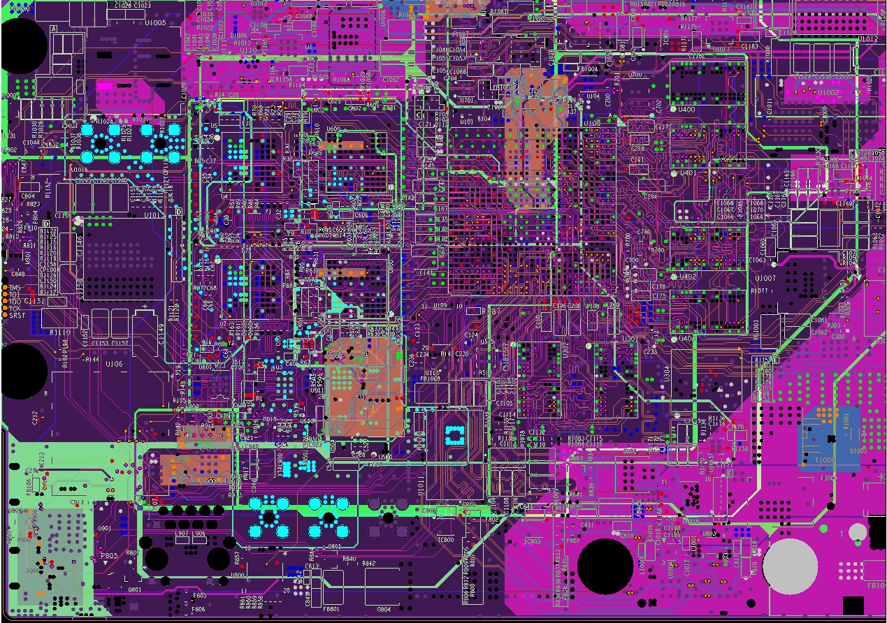
PCB Design Optimization: Line width and spacing meet manufacturing capabilities (conventional ≥0.1mm/0.1mm, high-density ≥0.08mm/0.08mm); pad design follows IPC-7351 standard, using teardrop design to reduce stress concentration; through-hole diameter ≥0.3mm, blind/buried holes adapt to high-density wiring and reduce PCB layers; avoid acute angle wiring (≥135°) to reduce etching defect risks.
Material and Process Adaptation: Select substrates according to product scenarios (ordinary FR-4 for consumer electronics, high Tg FR-4 for automotive electronics); surface treatment matches soldering processes (ENIG for fine-pitch components, HASL for cost control); solder paste thickness and stencil opening size adapt to component packages to avoid bridging or cold soldering.
Test Feasibility Design: Reserve test points (spacing ≥2.54mm, quantity meets ICT/FCT test needs); reserve X-Ray inspection space in key areas (BGA/QFN); silk screen is clear and accurate, avoiding covering pads or test points.
Component Selection: Prioritize standardized and generalized components to reduce custom parts; avoid special-shaped components and fine-pitch components (unless necessary) to reduce placement difficulty; separate layout of heavy and light components (heavy components near PCB edges or brackets to reduce warpage).
Layout Optimization: Concentrated layout of functional modules to shorten signal links; separate placement of SMT and THT components to adapt to hybrid SMT/THT processes; reserve assembly tool operation space (≥5mm) to avoid component interference.
Assembly Process Design: Adopt the principle of "positioning first, then fixing" and design guiding features; prioritize snaps and bonding instead of screws to reduce assembly steps; error-proof design (such as component polarity marks, assembly stops) to avoid reverse or wrong assembly.
The core goal of Layboard EQ is to balance the electrical performance, process feasibility, and heat dissipation efficiency of circuit layout, reducing post-debugging and rework costs.
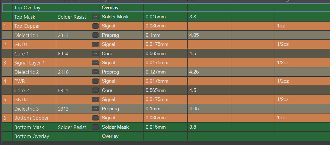
Lamination design must balance the matching of rigid-flex characteristics, signal integrity, and mechanical strength to avoid problems such as delamination and warpage.
Prioritize simplified part counts, standardized interfaces, and accessible assembly paths in DFA. Align designs with automated/manual processes to cut time, lower costs, and boost PCBA reliability.
 Add: 803-804, Hisee International Commercial Center, Dongbin Road, Nanshan District, Shenzhen, China
 Tel: 0086-755-2664 8283
 E-mail: info@fully-hong.com


Copyright ©2025 Fully Hong Electronics Co.,Ltd. |A Professional And Reliable EMS/PCBA Partner.
