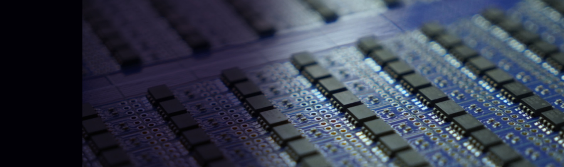
Deliver micron-level component placement,
support 01005/0201 miniaturized parts,
and ensure consistent quality across prototype to mass production runs.
Our SMT PCB Assembly services offer end-to-end support for all your electronic manufacturing needs, combining advanced automation with decades of engineering expertise to bridge the gap between design and production. We start with a free DFM (Design for Manufacturability) review to optimize your PCB layout for assembly efficiency and defect reduction, followed by rigorous IQC checks to verify component authenticity and compliance with specifications. Equipped with high-speed placement machines (±25μm accuracy), we handle pure SMT, hybrid SMT-THT, and high-density interconnect (HDI) assemblies, with flexible capacity to fulfill low-volume prototype runs and high-volume production orders without compromising on quality or lead times.
Contact us


●PCB layout optimization for SMT compatibility. (With EQ file.)
●Component sourcing and counterfeit prevention.
(Material verification, moisture-sensitive component storage.)
●Custom stencil fabrication.
(Laser-cut stainless steel, aperture design for fine-pitch components.)

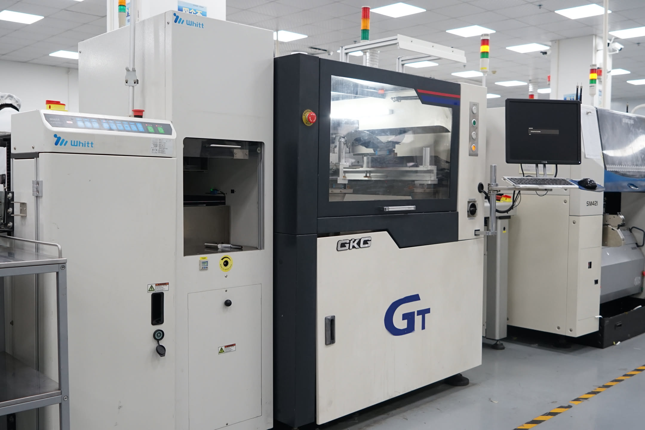
●Stencil printing with laser alignment for precise deposition
●In-line SPI (Solder Paste Inspection) for real-time paste volume and alignment verification.
●Common issues: paste slumping, bridging, and their prevention measures.


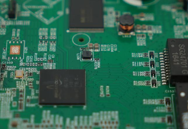
●Machine capabilities: 90,000CPH (components per hour), ±25μm placement accuracy.
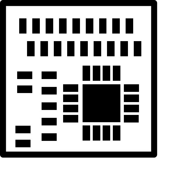
●Support for component types: 01005/0201 passives, QFN/BGA/CSP ICs, connectors, PoP packages.
●Vision system alignment for ultra-small component.


●Dual-Wave Reflow Soldering Oven with 12 Temperature Zones.
●Temperature profiling optimization for different component packages.
●Solder void rate control below 5% for critical applications.


●AOI (Automated Optical Inspection) for surface defect detection. (99.98% accuracy.)
●X-Ray inspection for hidden defects in BGAs, QFNs, and other leadless packages.
●First Article Inspection (FAI) to validate production setup.


This dedicated process acts as a final quality assurance measure, addressing rare, inspection-detected anomalies (defective solder joints, misaligned components) to ensure all delivered assemblies meet IPC quality requirements and your performance expectations.
| ltem | Capability |
|---|---|
| PCB Layers | 1-50 |
| Min.Width/Space | 3/3 mils |
| PCB Min. Hole Dia. | 0.1mm |
| Solder Printer Accuracy | ±0.035mm(±0.025mm) |
| Hi-speed mounterAccuracy | ±0.035mm(±0.025mm) |
| Max.BGA Size | 50mm*50mm |
| Min.BGA Dia. | 0.14 mm |
| PCB Size | 45x45mm — 510x500mm |
| Min.SM. Bridge | 0.1mm |
| PCB Thickness | 0.2-5.0mm |
| Max.Stencial Size | 740X740mm |
| Min. Component Size | 01005 |
| Multi-function Mounter Accuracy | ±0.035mm(±0.025mm) |
| Min.IC Pitch | 0.3mm |
| Min.BGA Pitch | 0.2mm |
| IC Package | DIP, SOP, SOJ, PLCC, QFP, QFN, BGA, POP etc |
| PCB Finish | HASL lead free, OSP, ENlG, Immersion Tin etc |
Full automation, ultra-fine printing capability, and strict process consistency—laying the groundwork for defect-free solder joints and high-yield PCBA manufacturing.
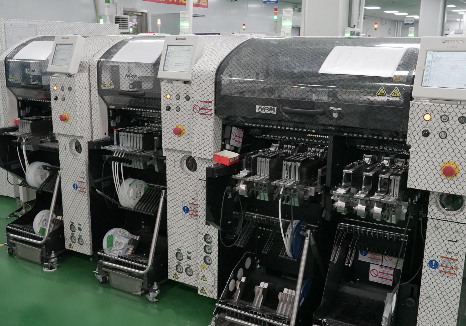
High-speed (90k+ CPH), ultra-precise (±25μm), and fully versatile—handle any component, any PCB, and elevate your SMT assembly efficiency.
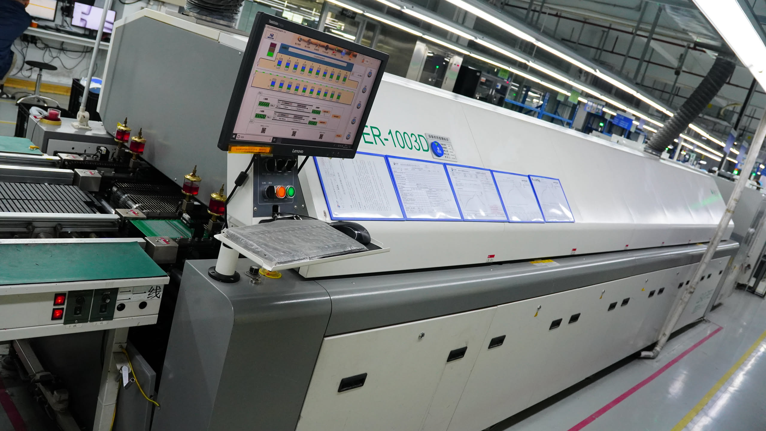
Dual-Lane Efficiency + Precision Thermal Control, Flawless Soldering10–12 zones, ±1℃ accuracy, nitrogen-ready—boost throughput with parallel production, elevate SMT soldering quality.
 Add: 803-804, Hisee International Commercial Center, Dongbin Road, Nanshan District, Shenzhen, China
 Tel: 0086-755-2664 8283
 E-mail: info@fully-hong.com


Copyright ©2025 Fully Hong Electronics Co.,Ltd. |A Professional And Reliable EMS/PCBA Partner.
