Let Your Design Come to Reality, Make Circuits More Reliable, Make Innovation More Free
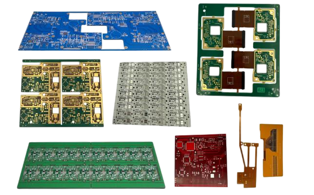
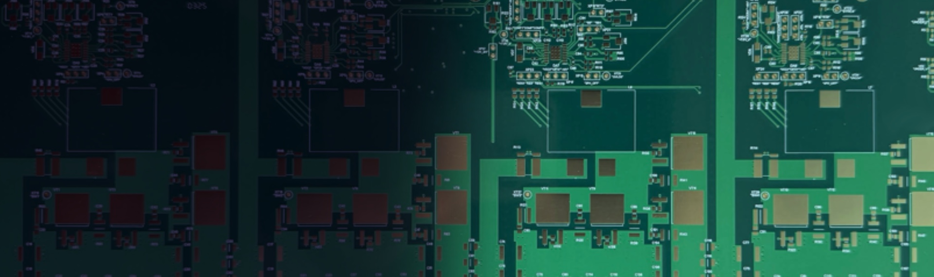
As a leading PCB manufacturer in China, Fully Hong boasts extensive experience and profound expertise spanning the entire PCB lifecycle — from design and manufacturing to testing and after-sales support. All processes are completed in our ISO-certified manufacturing facilities. Quality is our top priority, and every circuit board undergoes rigorous quality control inspections prior to shipment. We specialize in the production of a comprehensive range of printed circuit boards, including PCB prototypes, FR4 PCBs, double-sided PCBs, aluminum-based PCBs, high-frequency PCBs, and HDI PCBs.


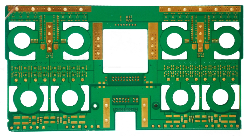
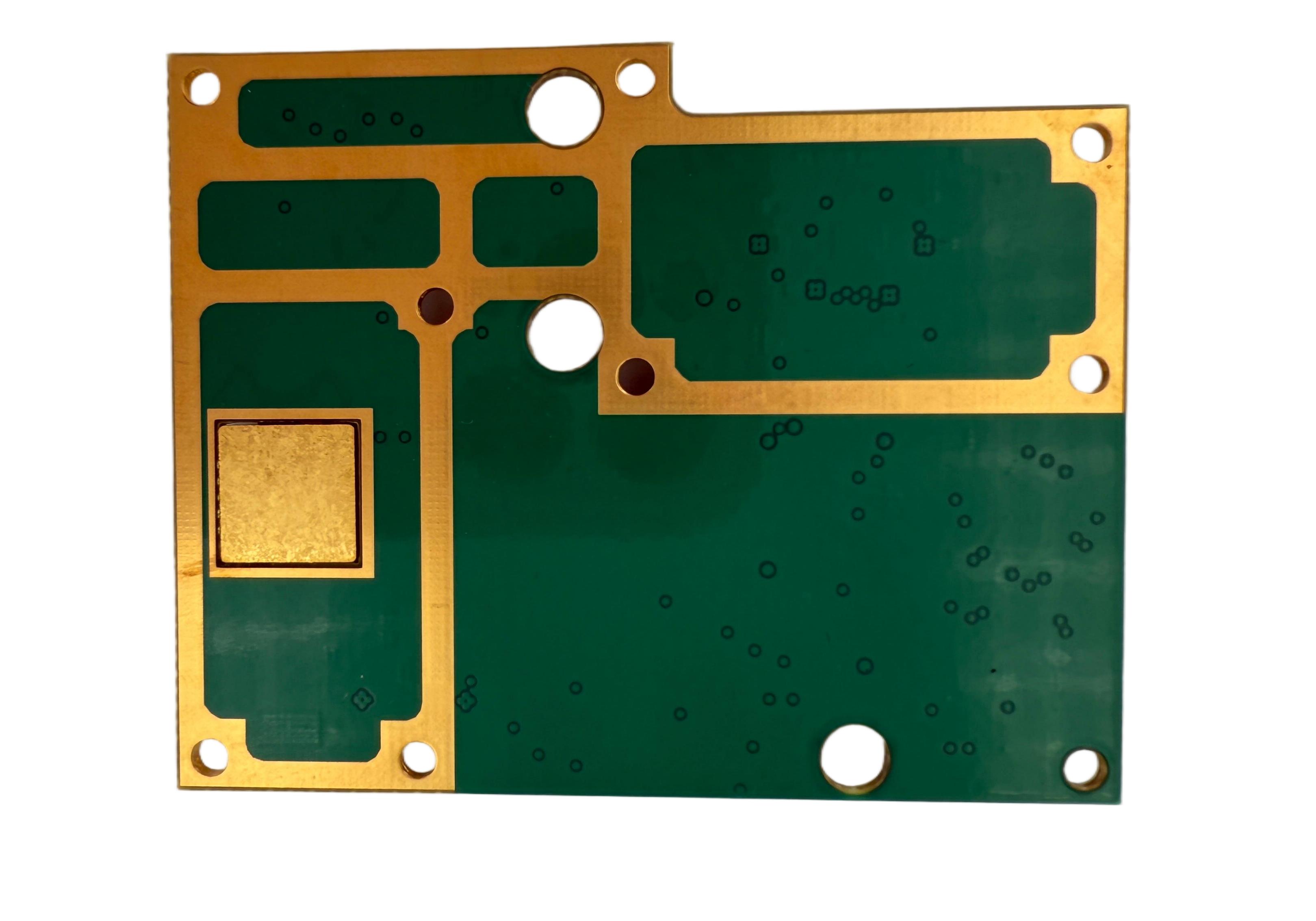
Covers FR4 standard rigid PCBs, high Tg rigid PCBs (Tg≥130℃/150℃), metal-based rigid PCBs (aluminum-based, copper-based, iron-based), high-frequency rigid PCBs (substrates such as PTFE and Rogers). Supports customization of 1-50 layers.


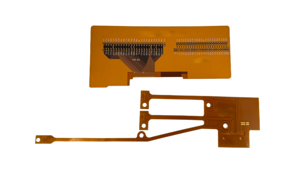
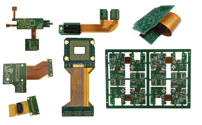
Flexible PCB/FPC: Adopts flexible substrates such as polyimide (PI), supports customization of single/double-sided and multi-layer flexible PCBs. Features bendability and light weight.


Integrates the mechanical support of rigid PCBs and the bendability of flexible PCBs, supports various stack-up structure designs, and can realize circuit interconnection in complex assembly spaces.


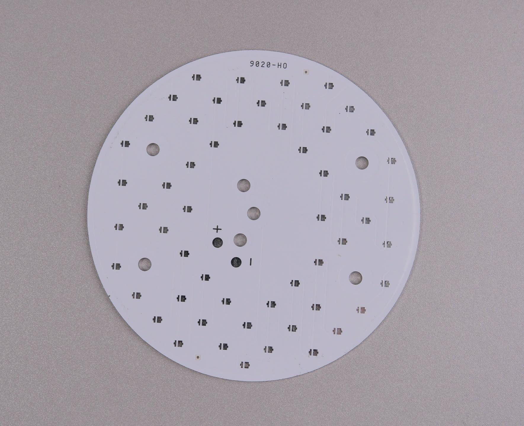
Focus on customization for high heat dissipation needs, subdivided into three core products. Aluminum-Based PCB, Copper-Based PCB, Iron-Based PCB.
Polymer Over Filled Via, Provides resin hole filling + surface copper/tin plating services, enabling hole flattening. Suitable for high-density routing and high-frequency signal transmission scenarios, improving PCB reliability and aesthetics.
Supports laser drilling process. Suitable for high-density integration needs of high-end smartphones, tablets, servers, etc.


Precisely controls the line impedance value with a stable tolerance of ±10% (±5% for high-precision requirements), supports customization of various impedance types such as differential impedance and single-ended impedance.
Supports customization of copper foil thickness from 3oz to 10oz, with low resistance, high current-carrying capacity and excellent heat dissipation.


Provides pre-design services such as Design for Manufacturability (DFM) analysis, schematic optimization, PCB layout design, and Gerber file review & optimization to reduce production risks.


Covers electrical performance and reliability tests such as flying probe testing, bed of nails testing, impedance testing, temperature cycle testing, AOI, and damp heat testing to ensure product quality.


Provides professional reverse engineering, schematic restoration, BOM list sorting, and PCB file reconstruction services. Supports cloning needs of various conventional boards, high-frequency boards, rigid-flex boards, etc.


Supports small-batch rapid prototyping (24-48 hour delivery) and medium-to-large batch mass production with a monthly capacity of up to 1 million ㎡, meeting the needs of different order sizes.


Conduct Design for Manufacturability (DFM) analysis to check whether line width, hole diameter, etc. meet process capabilities, and selects raw materials such as substrates and copper-clad laminates according to requirements.


Cut large copper-clad laminates into substrates that meet production dimensions through cutting equipment to ensure substrate dimensional accuracy and flat edges.


PRETREAT, LAMINATION, EXPOSURE, DEVELOPING, ETCHING, STRIP, PUNCH, Inner Layer AOI.


Align inner layers, Prepreg and outer copper foil as preset, bond them into one piece via high-temperature and high-pressure curing of Prepreg; then mill edges and drill positioning holes for subsequent alignment.


Use mechanical (≥0.15mm) or laser (<0.15mm, for HDI blind/buried holes) drilling to make through, blind or buried holes; perform desmearing after drilling for PTH preparation, with accuracy up to ±0.05mm.


Plating Through Hole, deposit thin copper (0.3-1μm) on hole walls via chemical copper plating, then thicken to 20-30μm by electroplating to ensure reliable inter-layer connection.


Similar to inner layer processing; form preliminary electroplating circuit patterns via film lamination, exposure and development.


Electroplate copper (and optional tin for protection) on developed outer circuits, strip film, etch excess copper, and remove tin to form complete outer circuits.


Apply photosensitive solder mask ink, expose and develop to expose pads; screen print component marks and polarity symbols for easy mounting and maintenance.


Treat pads to improve solderability and oxidation resistance; common processes include HASL, ENIG, Immersion Tin/Silver, OSP, selected by application scenario.


Cut PCB into desired shape (V-cut, special shape) via CNC milling, and drill mounting holes simultaneously.


Conduct electrical tests (flying probe, bed of nails) and AOI inspection, with manual sampling; clean PCBs, package in vacuum for moisture protection, attach quality reports and labels before shipping.
Fully Hong has been engaged in PCB manufacturing more than 20 years and is a reliable Chinese PCB manufacturer. We have a strong production capacity and can produce various PCBs from standard PCBs to Double Sided PCBs, Multilayer PCBs, High TG PCBs, etc.
| Layer | 1-50 layer |
| Via Types | Through-hole, Blind hole, Buried hole, Stacked via (HDI), Step via |
| Via Density | Up to 500000 vias per square meter (Normally 100000 vias per square meter) |
| Material | FR-4 (Tg 130℃/150℃/170℃), PTFE, Rogers 4350B/4003C, Arlon, Aluminum, Copper, Iron, Polyimide (PI), Polyester (PET) |
| Board Thickness | 0.2mm-8mm |
| Thickness Tolerance | ±0.1mm (Board Thickness<1.0mm); ±8% (Board Thickness>1.0mm); |
| Bow & Twist | 0.75% |
| Max. finished board side | 610mm×1050mm for mass production |
| MAX. Core Thickness | 6OZ |
| Impedance value tolerance | ±5% |
| Min. Mechanical Drill size | 0.15mm; Depth ratio up to 10:1 |
| Max. Mechanical Drill size | 6.5mm |
| Finished hole size tolerance for PTH | ±0.045mm |
| Finished hole size tolerance for NPTH | ±0.025mm |
| Min. BGA Pitch (1 OZ) | 0.76mm |
| Maximum times of Lamination | 3 |
| HDI Technology | YES |
| Backdrill Capability | YES |
| POFV or VIPPO | YES |
| Embedded Coin | YES |
| Inlay PCB inside the board | YES |
| Segmented/Graded gold finger gold finger | YES |
| Rogers+FR4 hybrid construction | YES |
| Edge plating (Half via) | YES |
| Solid copper filling for microvias | YES |
| Epoxy filling for microvias | YES |
| min. line spacing | 0.075mm(3mil) |
| Min. Pad to Pad Spaces | 0.24mm |
| Min. Annular Ring | 0.15mm |
| Tolerance of circuit width | ±0.02mm |
| Min distance from copper to outline | 0.2mm |
| Buried Vias (Min. Size) | 0.15mm |
| Blind Mechanical Vias (Min. Size and Tol.) | 0.15mm±0.076mm |
| Press-Fit Hole Tolerance | ±0.05mm |
| Surface Finish/Treatment | HASL/HASL-LF, lmmersion,Immersion Silver, Immersion Tin, OSP, ENENPIG... |
| Solder Mask Color | Black/White/ Green / Blue / Yellow/ Red... |
| Hi-Pot Test | YES |
| Inductance Test | YES |
| ET Tester Types (Grid or Flying Probe) | YES |
| IST | YES |
 Add: 803-804, Hisee International Commercial Center, Dongbin Road, Nanshan District, Shenzhen, China
 Tel: 0086-755-2664 8283
 E-mail: info@fully-hong.com


Copyright ©2025 Fully Hong Electronics Co.,Ltd. |A Professional And Reliable EMS/PCBA Partner.