Professional PCB Cloning & Technology Upgrade Service Provider
PCB Reverse Engineering (also known as cloning) is a key technical service in the field of electronic manufacturing and R&D. It conducts comprehensive analysis of existing PCB boards through professional technical means to restore core design information such as circuit layout, stack-up structure, and component parameters, and finally generates standardized design files directly usable for production. Its core value lies in providing enterprises with efficient technical breakthrough and cost control solutions: for new product R&D, it can quickly grasp industry technical trends through competitive product reverse engineering analysis, shortening the R&D cycle. For old equipment maintenance, it can accurately replicate out-of-production PCB boards, avoiding production line paralysis or equipment scrapping caused by the lack of core components; For small and medium-sized innovative enterprises, it can greatly reduce the threshold and risk of independent R&D. In terms of technical capability, we have industry above-average full-scenario reverse engineering strength, covering various complex PCB structures such as double-sided boards, multi-layer boards, HDI boards, blind/buried via boards, and flexible boards.
Contact us


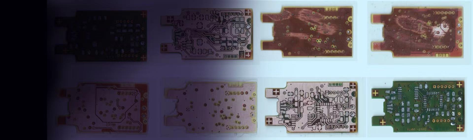
Adopt a combined technical scheme of \"non-destructive testing + precision scanning\" to realize layered analysis and data extraction of all types of PCBs, conduct comprehensive scanning of the top, bottom and inner layers of PCBs, and optimize image contrast through professional image processing software to ensure clear visibility of copper film circuits. For multi-layer boards, a combined process of \"layered scanning + chemical etching\" is adopted to analyze the inner layer signal logic and power distribution layer by layer from outside to inside, accurately restoring special process structures such as blind/buried vias and back drilling. Finally, output full-format production files such as Gerber, Drill, and ODB++, compatible with mainstream EDA software such as Altium Designer, Eagle, and PADS, supporting direct docking with production.


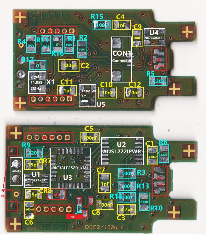
Complete precise identification and parameter measurement of all board components through professional equipment such as XRF spectrometers and bridge testers: can identify precision SMD components such as QFN and BGA, solve problems such as blurred, worn or out-of-production component silk screens, and accurately measure parameters such as resistors, capacitors, and inductors. Output a standardized Excel format BOM list, including complete information such as component position numbers, packages, brands, parameters, and procurement links, supporting customers to place orders directly. At the same time, provide localized substitution and cost reduction optimization solutions.


Provide full-dimensional design upgrade services based on cloning: for defects such as insufficient heat dissipation, severe electromagnetic interference (EMI), and impedance mismatch of the original board, re-plan component layout and circuit routing through thermodynamic simulation and signal integrity analysis to improve product stability. Support functional expansion and development, on the basis of retaining the original core functions, add interface modules such as USB, WiFi, and 4G, or upgrade chip models to achieve performance improvement, helping customers form a differentiated competitive advantage. At the same time, provide compatibility design guarantee to ensure that the modified PCB is fully compatible with the original system (firmware, shell, connector), avoiding secondary development risks.


Provide one-stop service of \"cloning - prototyping - testing - mass production\": cooperate with high-quality PCB manufacturers to realize 24-hour rapid prototyping, supporting the production of prototypes of special materials such as rigid-flex boards, high-frequency boards, and heavy copper boards. After the prototype is completed, conduct full-function testing, including DRC design rule check, flywire testing, quiescent current testing, temperature and humidity environment testing, etc., to ensure that the prototype performance is completely consistent with the original board. Subsequently, it can dock with PCBA SMT factories, provide mass production technical support, follow up the production progress throughout the process, and ensure delivery quality and cycle.
Repair damaged PCB boards of old equipment such as PLCs and inverters, replicate out-of-production core components, and avoid production line paralysis; analyze the design of competitive controllers and quickly launch compatible products to seize the market.
Replicate the PCB design of popular products such as smart watches and TWS earphones, shortening the R&D cycle to within 1 month; reduce production costs and improve product price competitiveness through BOM optimization and design improvement.
Analyze the PCB design of modules such as ECUs, sensors, and on-board chargers (OBCs) to provide alternative parts for the after-sales market; upgrade the functions of in-vehicle entertainment systems, adding new features such as CarPlay and 4G networking.
Conduct reverse analysis on imported monitors and ultrasonic instrument PCBs to realize the localization of core components.
 Add: 803-804, Hisee International Commercial Center, Dongbin Road, Nanshan District, Shenzhen, China
 Tel: 0086-755-2664 8283
 E-mail: info@fully-hong.com


Copyright ©2025 Fully Hong Electronics Co.,Ltd. |A Professional And Reliable EMS/PCBA Partner.
