PCB Prototyping Faster, Innovation R&D Assured, One-Stop Stencil Coordination Service
PCB Prototype is a crucial link in the electronic product R&D process, directly determining the efficiency of product concept verification and the speed of innovation iteration. With a mature local production layout and efficient order response mechanism, we provide high-reliability and fast-response PCB prototype services for electronic R&D enterprises and engineers worldwide, covering the prototype needs of all categories such as rigid boards, flexible boards, rigid-flex boards, and HDI boards, adapting to diverse application scenarios from consumer electronics to industrial control and medical electronics.


Provide free EDA design tool support and DFM (Design for Manufacturability) audit services, real-time detection of more than 20 design hazards (such as line width and spacing, hole position deviation, pad size, etc.), and provide optimization schemes to improve design success rate.


Set up a professional technical team to provide 24/7 online consulting services to answer technical questions such as PCB design, material selection, and stencil matching.


Support design optimization and secondary prototyping after sample test feedback, provide reasonable after-sales guarantee schemes; bulk orders can enjoy exclusive customized services and preferential prices.
As a core supporting link of PCB prototyping, we provide full-process SMT stencil design and manufacturing services, strictly following the IPC-7525A international standard to ensure the quality of solder paste printing and placement reliability, helping customers quickly advance the subsequent assembly process.
Efficient Delivery Guarantee
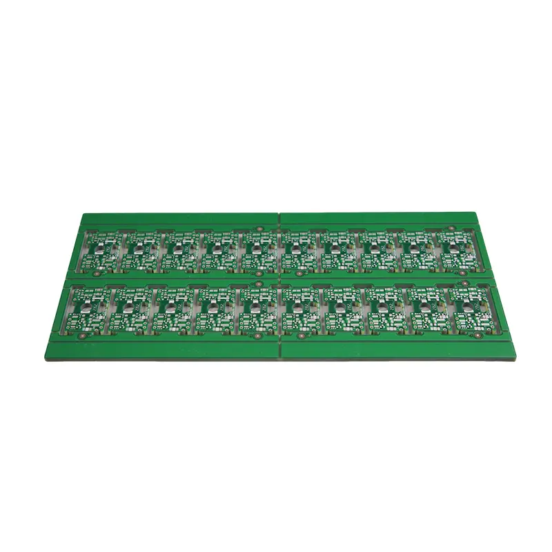
Relying on the mature PCB industrial supporting advantages, we have built an efficient delivery system that meets market needs, focusing on the rapid response of small and medium batch prototyping: for the industry's mainstream FR-4 conventional single/double-sided boards, if documents are confirmed and payment is completed, delivery can be achieved within 24 hours. For 4-8 layer board prototyping, delivery can be achieved within 72 hours.
Comprehensive Practical Material Supply
Covering mainstream PCB substrates in the industry, accurately matching most R&D and small-batch production needs: for conventional R&D scenarios, cost-effective standard substrates such as FR-4 (Tg 130℃/140℃) and CEM-1 are prioritized, with stable and sufficient supply, which can meet the basic needs of daily consumer electronics, ordinary industrial control and other fields.
Stable and Reliable Precision Control
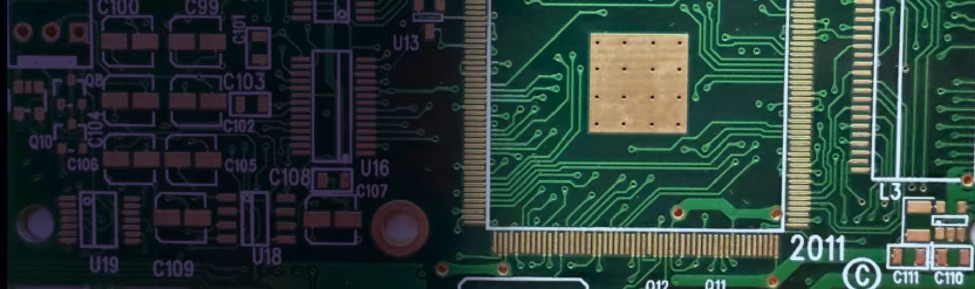
Adopting mature production equipment and processes in the industry to ensure that the sample precision meets the actual assembly and testing needs: the minimum line width and spacing can stably reach 3/3mil, fully adapting to the design requirements of most R&D products; for high-density design needs, it can support 2mil line width and spacing processing, and ensure precision stability through strict process control. All prototyped products undergo strict quality inspection, including core items such as visual inspection, continuity testing, and insulation resistance testing, to ensure no basic problems such as short circuits and open circuits.
Practical Cost Control Plan
Starting from the actual needs of customers, we provide down-to-earth cost control solutions to help customers save R&D expenses: by optimizing the panelization plan, on the premise of ensuring the integrity of samples, the utilization rate of substrates is improved, and the cost of a single sample can be reduced. For small and medium batch prototyping customers, a step-by-step quotation is launched, with more discounts for larger orders. At the same time, standardize the production process to reduce material waste in the production process and lower unnecessary processing costs; do not forcibly recommend high-priced materials, but recommend suitable cost-effective substrates according to the customer's actual use scenarios. All quotations are open and transparent with no hidden fees, allowing customers to have a clear understanding of the cost.
 Add: 803-804, Hisee International Commercial Center, Dongbin Road, Nanshan District, Shenzhen, China
 Tel: 0086-755-2664 8283
 E-mail: info@fully-hong.com


Copyright ©2025 Fully Hong Electronics Co.,Ltd. |A Professional And Reliable EMS/PCBA Partner.
