Precise Interconnection, Ultimate Performance
Professional HDI PCB Customization, Driving Global Clients' Technological Breakthroughs
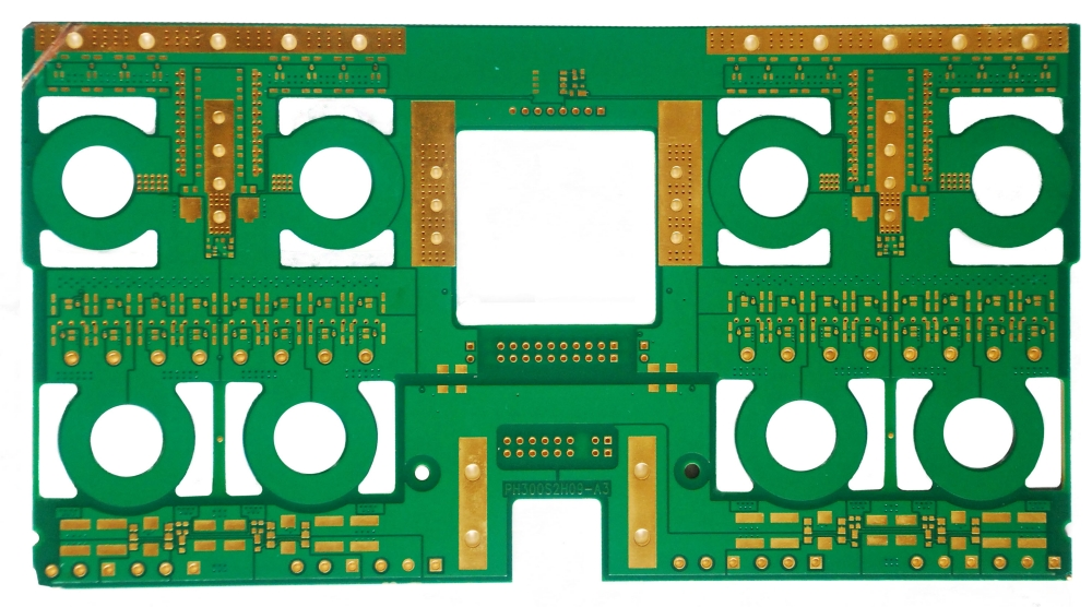
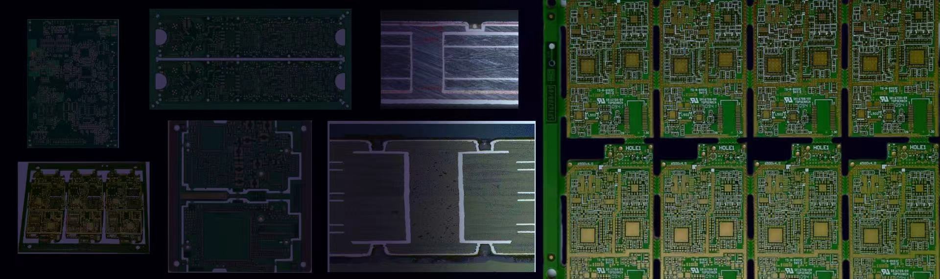
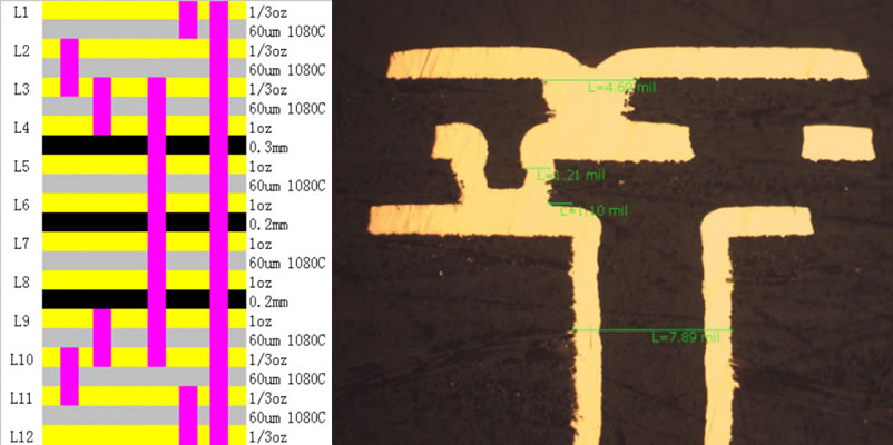
High Density Interconnect Printed Circuit Board (HDI PCB) is a cutting-edge product in the modern electronic manufacturing industry. It is manufactured using microvia, fine line, and thin dielectric materials, achieving high-density interlayer interconnection through blind/buried vias and Build-up processes. Its core features include microvias as small as 75-100μm, line width/spacing down to 75/75μm, and interlayer interconnection density increased by more than 30% compared to traditional PCBs, completely breaking through the physical limitations of ordinary PCBs in wiring density and space utilization. With higher integration, better signal integrity, and smaller size, HDI PCB has become the core carrier for high-performance and miniaturized designs in 5G communication, high-end consumer electronics, automotive ADAS and other fields.
Contact us


Uses laser drilling with minimum aperture up to 75μm, combined with Build-up process to realize direct interconnection between any layers, eliminating the space occupation of traditional through-hole stubs on the board surface.

Supporting 75/75μm ultra-fine lines and greatly increasing wiring density per unit area.


Uses high-performance substrates and Resin Coated Copper (RCC) to reduce signal transmission loss and improve interlayer bonding force.

Supports 1+N+1, 2+N+2 and Any Layer HDI structures to meet circuit design requirements of different complexities.


Can accommodate 3 times more circuit nodes than traditional PCBs in the same area.


Microvia technology reduces signal transmission path, low-loss substrates (Df≤0.005) reduce high-frequency signal attenuation, and differential impedance control accuracy can reach ±5Ω


Helps reduce terminal product, perfectly adapting to miniaturized product designs such as smartphones and wearable devices.


Any Layer HDI technology provides engineers with maximum design freedom, enabling customized layouts such as power ground network optimization and high-speed signal isolation.
HDI PCB has deeply penetrated into high-end fields with strict requirements for circuit integration and performance, becoming the core support for promoting electronic equipment upgrades:
5G Communication Equipment: 5G base stations, millimeter-wave radars, optical modules, etc., meeting the needs of high-frequency signal transmission above 28GHz.
High-End Consumer Electronics: Flagship smartphones, smart watches, VR/AR devices, realizing 15% reduction in motherboard area and 20% increase in integrated functions.
Automotive Electronics: ADAS advanced driver assistance systems, in-vehicle infotainment systems, BMS battery management systems, supporting high-speed data transmission above 10Gbps and reducing data processing latency from 50ms to 20ms.
Medical Electronics: Portable electrocardiographs, blood glucose analyzers, endoscopes, etc., realizing high-precision signal acquisition and transmission in limited space with measurement error controlled within ±2%.
Aerospace and Military: Satellites, drones, radar equipment, meeting high-performance and lightweight requirements in extreme environments.
High-Performance Computing: AI servers, data center switches, supporting high-density chip packaging and high-speed data interaction.
 Add: 803-804, Hisee International Commercial Center, Dongbin Road, Nanshan District, Shenzhen, China
 Tel: 0086-755-2664 8283
 E-mail: info@fully-hong.com


Copyright ©2025 Fully Hong Electronics Co.,Ltd. |A Professional And Reliable EMS/PCBA Partner.
