The integrated core carrier of high-end electronic equipment
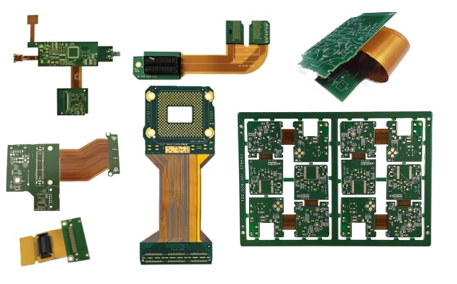
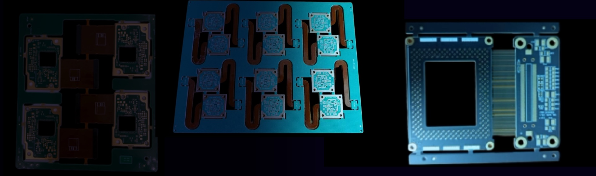
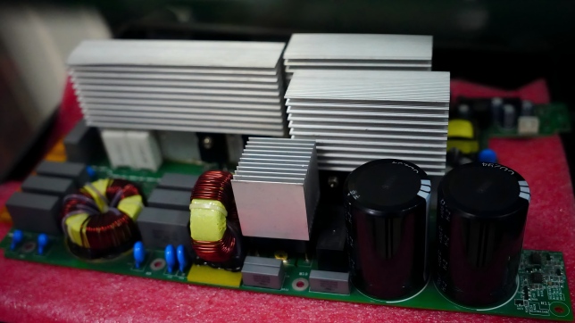
Rigid-Flex PCB Assembly is a high-end PCBA process that integrates the structural stability of Rigid PCB and the bending adaptability of Flex PCB. Through SMT, THT, or hybrid processes, electronic components are mounted on an integrated substrate. After soldering, reinforcement, inspection, and post-processing, it forms a functional module that can realize 3D spatial layout, withstand dynamic bending, and adapt to narrow and special-shaped spaces.
With the accelerating trends of consumer electronics miniaturization, automotive electronics intelligence, and medical equipment precision, it has upgraded from a high-end niche process to a rigid demand technology.


Foldable mobile phones (hinge area circuits, camera modules)
smart watches (strap circuits, sensor integration)
wireless earphones (battery connection, audio modules)
AR/VR equipment (head-mounted structure wiring)


ADAS systems (radar, camera connection)
Battery Management System (BMS, battery pack wiring)
Smart cockpit (central control screen, ambient light circuit)
Automotive sensors


Implantable medical devices (pacemakers, neurostimulators)
Wearable monitoring devices (blood glucose/ECG patches)
Medical endoscopes (imaging module circuits)


Satellite communication equipment (lightweight circuits)
Aviation instruments (special-shaped structure adaptation)
UAVs (sensor and flight control connection)
· Substrate Adaptation: FR-4 (conventional scenarios), high Tg FR-4 (high-temperature scenarios, Tg≥170℃) or ceramic-filled materials (high-frequency scenarios) are used for rigid areas; polyimide (PI, temperature resistance 260℃) is preferred for flexible areas, polyester (PET, temperature resistance ≤150℃) for economical scenarios, and PTFE (dielectric constant ≤2.1) for high-frequency scenarios.
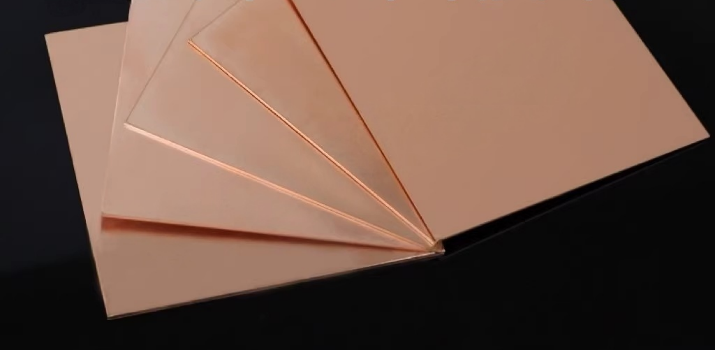
· Conductive Layer Selection: Rolled annealed (RA) copper foil (good ductility, bending resistance) is used for flexible areas, and electrodeposited (ED) copper foil (cost-controllable, suitable for static areas) for rigid areas. The copper foil thickness is 0.5-2 ounces (17-70μm), and 2-ounce thick copper is used for high-current areas.
· Adhesive and Lamination: Acrylic adhesive (good flexibility, temperature resistance 150℃) or epoxy adhesive (high temperature resistance 180℃, high rigidity) is selected, and adhesive-free laminates are used in high-end designs to reduce thickness; lamination configurations can be customized (2-layer rigid + 1-layer flexible, 4-layer rigid + 2-layer flexible, etc.), and the transition area requires continuous lamination design to avoid stress concentration.
The transition area is the core of the process, requiring smooth connection between rigid and flexible parts
· Circuit design: 45° bevel or arc wiring is adopted to avoid right angles, and wires are perpendicular to the bending line, evenly distributed to reduce stress concentration;
· Edge treatment: Stress relief grooves are set to remove burrs and prevent circuit breakage during bending;
· Reinforcement design: FR-4 or stainless steel stiffeners are pasted on the edge of the transition area to improve mechanical strength.
A segmented temperature control strategy is adopted to balance the soldering quality of the rigid area and the substrate tolerance of the flexible area
· Solder paste selection: Conventional solder paste is used for the rigid area, low-melting-point solder paste (Sn42Bi58, melting point 138℃) for the flexible area, and low-impedance solder paste for high-frequency scenarios;
· Temperature profile: Slow heating in the preheating stage, peak temperature of 180-200℃ for the flexible area with duration ≤30s, peak temperature of 245-260℃ for the rigid area, and gradient cooling in the cooling stage to reduce thermal stress;
· Positioning and fixing: Magnetic carriers or vacuum adsorption workbenches are used for fixation to ensure the flatness of the flexible area (flatness ≤0.1mm) and avoid placement offset.
· Reinforcement Process: FR-4, stainless steel, or polyimide stiffeners are pasted on component mounting areas, connector interfaces, and rigid-flex transition areas to improve load-bearing capacity and insertion force, with no bubbles or warpage between the stiffener and the substrate.
· Protection Treatment: The flexible area is coated with conformal coating or nano waterproof coating, and EMI shielding layer is added in high-frequency areas; Plasma cleaning is used to remove soldering residues, improve coating adhesion.
Develop thinner (flexible layer thickness ≤25μm), bend-resistant (million-cycle), and high-thermal-conductivity substrates; promote liquid crystal polymer (LCP) and carbon nanotube-reinforced materials to improve high-frequency performance and mechanical strength; the application ratio of adhesive-free laminates and halogen-free environmentally friendly materials will increase to 52%.
Introduce AI visual inspection (defect recognition rate ≥99.5%) and digital twin process simulation (simulate bending stress and welding deformation in advance); build a full-process digital management and control platform to realize traceability of materials, processes, and test data.
Realize integrated assembly of "rigid-flex circuit + sensor + battery + antenna + heat dissipation module"; develop embedded resistor and capacitor technology to reduce the number of components and improve integration; high-frequency and high-speed rigid-flex boards (line width/spacing ≤50μm) become mainstream.
 Add: 803-804, Hisee International Commercial Center, Dongbin Road, Nanshan District, Shenzhen, China
 Tel: 0086-755-2664 8283
 E-mail: info@fully-hong.com


Copyright ©2025 Fully Hong Electronics Co.,Ltd. |A Professional And Reliable EMS/PCBA Partner.
