Bear High Current, Achieve Efficient Heat Dissipation - Heavy Copper PCB Ensures High-Power Future
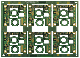
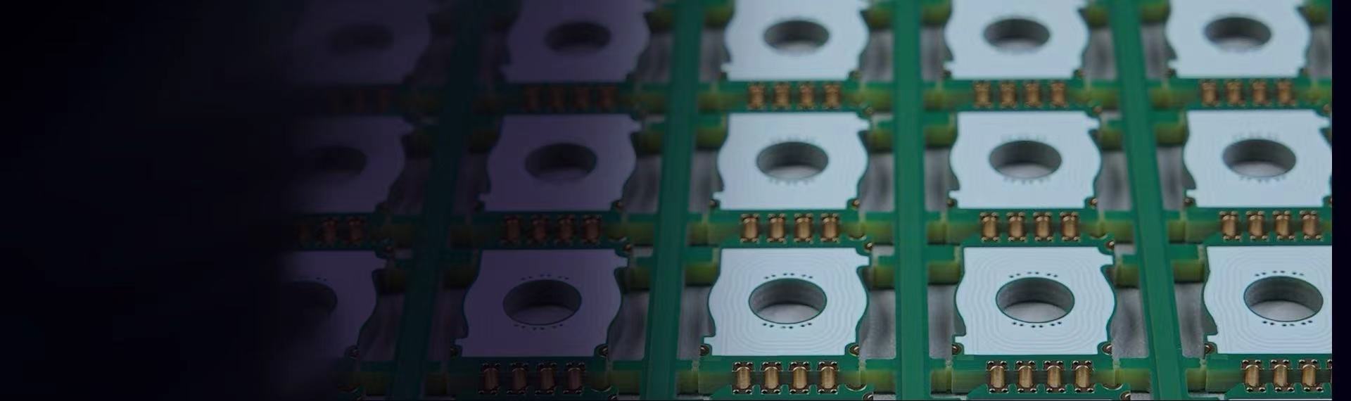
Heavy Copper PCB refers to a type of special printed circuit board that achieves significantly thickened copper foil through special manufacturing processes. Compared with conventional consumer electronic PCBs (copper foil thickness 0.5-1 ounce, only suitable for low current requirements ≤ 1A), Heavy Copper PCB is not a simple thickening of copper foil, but realizes the core functions of high current carrying capacity and efficient heat dissipation through the composite structure design of "circuit + plane" and the collaborative optimization of materials and processes, making it the core carrier for the stable operation of high-power electronic equipment.
Contact us

Heavy Copper PCB significantly reduces line resistance through the thickened copper layer, realizing stable transmission of large current. In a natural convection environment, the continuous current carrying capacity of 2-ounce copper foil (line width 2mm) can reach 5A, and 10-ounce copper foil (line width 2mm) can even reach 18A, fully meeting the needs of high-current scenarios above 100A such as industrial motor drives and new energy charging piles.

Heavy Copper PCB forms a \"natural heat sink\" through a large-area copper foil to quickly conduct device heat. A comparative experiment of an LED driver power supply shows that when the product using 2-ounce Heavy Copper PCB works at full load (50W), the chip junction temperature (85℃) is 20℃ lower than that of the 1-ounce board (105℃), meeting the automotive-grade reliability requirements. At the same time, Heavy Copper PCB can reduce or even eliminate the need for additional heat sinks.


The large-area ground copper foil can reduce the ground impedance (≤5mΩ), effectively reducing electromagnetic interference (EMI).The bonding force between the copper layer of Heavy Copper PCB and the substrate is stronger (peel strength ≥1.5N/mm), and its fatigue resistance under vibration and impact environments is more than 1.5 times that of conventional PCB.


Heavy copper PCBs can replace traditional wire harnesses, significantly reducing equipment volume. For example, the integrated DC/DC converter PCB can increase the power density to 50W/in³ through the copper layer embedded capacitor design.
New Energy Field:
Covers photovoltaic inverters, energy storage converters (PCS), new energy vehicle electric drive systems and charging pile modules. In photovoltaic inverters, 10-12oz Heavy Copper PCBs are used to carry large currents (200-500A) on the output side of the inverter, and cooperate with water-cooled heat dissipation structures to make the equipment run stably in high-temperature desert environments (60℃); energy storage converters adopt 8oz Heavy Copper PCBs to realize rapid switching of charging and discharging currents, reduce energy loss and improve energy storage efficiency.
Industrial Control Field:
Suitable for industrial frequency converters, servo drives, and PLC power modules. The power output unit of industrial frequency converters uses 6-8oz Heavy Copper PCBs, which can withstand output currents of 30-100A, solving the overheating problem of frequency converters during long-term high-load operation; the motor control circuit of servo drives uses 4oz Heavy Copper PCBs to improve the stability of signal transmission and reduce the impact of electromagnetic interference on control accuracy.
Automotive Electronics Field:
Includes on-board chargers (OBC), DC/DC converters, and battery management systems (BMS). Automotive OBCs adopt 6oz Heavy Copper PCBs to achieve 3.3kW-22kW power output in limited car space, meeting the fast charging needs of new energy vehicles; BMS uses 4oz Heavy Copper PCBs to realize real-time monitoring of battery cell voltage and current through precise current sampling circuit design, ensuring battery safety.
 Add: 803-804, Hisee International Commercial Center, Dongbin Road, Nanshan District, Shenzhen, China
 Tel: 0086-755-2664 8283
 E-mail: info@fully-hong.com


Copyright ©2025 Fully Hong Electronics Co.,Ltd. |A Professional And Reliable EMS/PCBA Partner.
