November 07, 2025|
 |
|
 Fully Hong
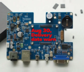
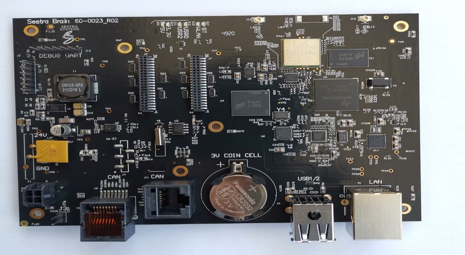
On a PCB, there are certain “special markings” that may seem insignificant at first glance but are, in fact, critical to ensuring smooth workflows from design to manufacturing, testing, and final delivery. Among them, test points and locating holes act as the “invisible heroes” that safeguard product functionality and production efficiency.
Have you ever faced prolonged debugging cycles due to poorly designed test points? Or reduced SMT yields because of inaccurate locating holes? This article reveals the critical role of test points, locating holes, and other special identifiers on PCBs—and explains their value across the entire PCB lifecycle.
PCB test points (Test Point) are conductive areas reserved for electrical testing during PCB manufacturing, assembly, and debugging. They typically appear as exposed pads, vias, or specially designed probe points, serving as the bridge between automated test equipment (such as ICT—In-Circuit Test ?) and the circuit on the board.
Functions and Types:
ICT (In-Circuit Test): Used to detect common manufacturing defects such as shorts, opens, or misplaced/missing components. Test points allow ICT systems to quickly locate faults, improving production efficiency and yield.
FCT (Functional Test): Test points act as access points for functional testing, simulating real-world operation to verify overall PCB performance.
Debugging & Repair: During product development or after-sales maintenance, engineers rely on test points for signal measurement and fault diagnostics.
Types of Test Points:
Pad-type test points: Using existing component pads or dedicated pads for testing.
Via-type test points: Using through-holes or blind vias as test points, often seen in high-density PCBs.
Probe pads: Special regions designed for spring probe contacts.
? Design Considerations: Test point size, spacing, placement, and coverage directly affect test efficiency. For example, test points should not be blocked by components, spacing should meet probe requirements (typically ≥50 mils), and they should cover key signal paths and power/ground nets. Optimized layouts can reduce debugging and troubleshooting time by up to 30%.

Locating holes and fiducial marks are special PCB features used for precise alignment during automated production and assembly. They ensure accuracy across multiple processes, from drilling to SMT placement.
Functions and Types:
SMT Placement: Automatic pick-and-place machines rely on locating holes or fiducials for orientation and alignment, ensuring accurate component placement.
Drilling & Profiling: Locating holes guide drilling and routing machines, guaranteeing that board dimensions and hole positions match design specifications.
Test Fixture Alignment: ICT/FCT test fixtures also use locating holes to ensure accurate probe-to-test-point alignment.
Common Types:
Tooling Holes: Non-plated holes at the board edge or designated areas, used for mechanical alignment throughout manufacturing and assembly. Typically placed in pairs or groups of three for orientation.
Fiducial Marks: Exposed copper pads (or solder mask openings) used by SMT vision systems for optical recognition. Global fiducials align the entire board, while local fiducials help align fine-pitch components like QFPs and BGAs.
? Accuracy Requirements: Tolerances for hole diameter, hole position, and fiducial shape/contrast directly affect recognition precision. Fiducials are usually 1–3 mm in diameter with clearly defined solder mask clearance, ensuring high visibility.

Beyond test points and locating holes, PCBs feature other markings that support communication and traceability across the product lifecycle.
Silkscreen Markings:
Component designators & polarity marks: Prevent errors in assembly and repair.
Company logos & product models: For branding and product identification.
Version numbers & date codes: For tracking and revision management.
Origin Marks: Indicate the PCB’s zero reference point or orientation.
Solder Mask Openings: Sometimes used for thermal dissipation, grounding, or special assembly requirements.
Impedance Control Indicators: Markings showing critical impedance-controlled traces, aiding production verification.
Stack-up Information: Complex multilayer boards may include simplified stack-up diagrams for manufacturing reference.
? These markings are more than just symbols on a board—they serve as a universal “language of communication” between design, manufacturing, testing, assembly, and repair. They enhance production efficiency, reduce errors, and ensure traceability. Neglecting them could result in costly rework, delays, or batch-level quality failures.

At [Fully Hong], we recognize the critical value of every PCB marking. Our professional team combines deep design expertise with extensive manufacturing and testing experience, ensuring your product is optimized for both quality and efficiency from the very beginning.
✅ DFM Excellence: Comprehensive Design-for-Manufacturability analysis ensures test points, locating holes, and fiducials fully comply with IPC standards and automated production requirements.
✅ Advanced Testing: With in-house ICT/FCT equipment and strict QC processes, we maximize the utility of test points to guarantee electrical and functional reliability.
✅ Precision Manufacturing: High-accuracy equipment ensures locating holes and fiducials are processed with exceptional precision, delivering outstanding SMT yields.
✅ End-to-End Solutions: From PCB design and fabrication to component sourcing, PCBA assembly, and testing, [Fully Hong] offers a complete one-stop service—saving you time, cost, and effort.
Your product’s success depends on attention to detail. Contact [Fully Hong] today to discover how precision PCB design and manufacturing solutions can improve your product reliability and market competitiveness!
 Add: 803-804, Hisee International Commercial Center, Dongbin Road, Nanshan District, Shenzhen, China
 Tel: 0086-755-2664 8283
 E-mail: info@fully-hong.com


Copyright ©2025 Fully Hong Electronics Co.,Ltd. |A Professional And Reliable EMS/PCBA Partner.

 Previous