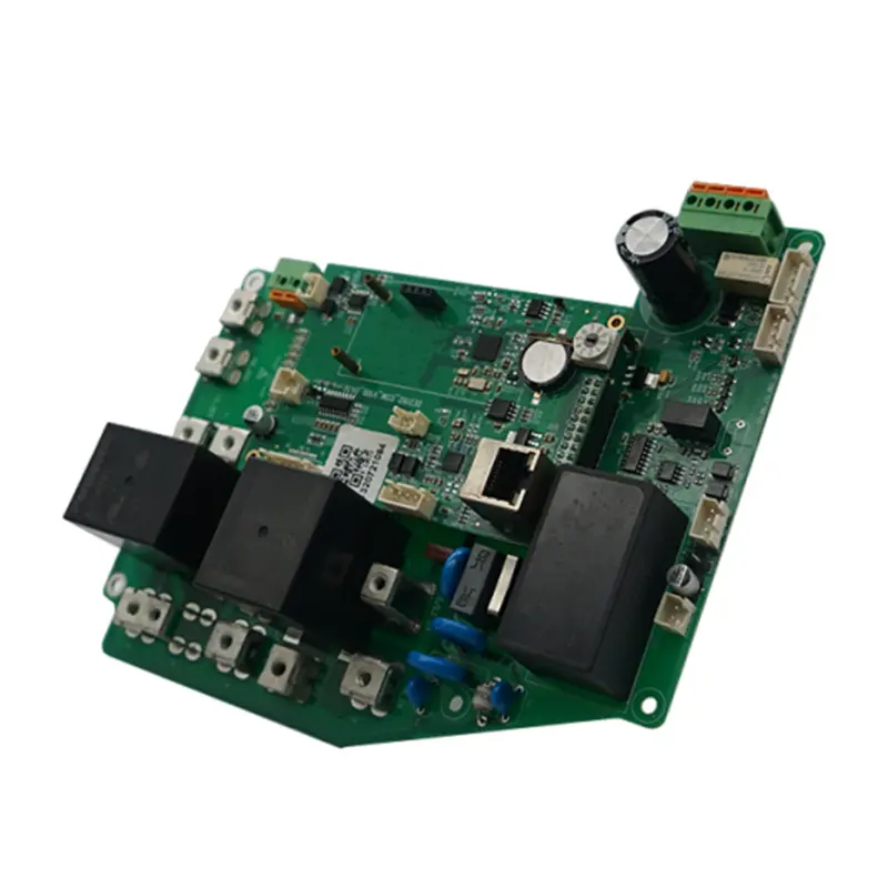


The Double-Sided PCBA for Renewable Energy Applications is engineered for robust performance and extreme reliability in demanding green energy systems. Utilizing advanced FR-4 High-TG (170°C) material and a substantial 2 oz (70µm) copper thickness, this board ensures superior heat resistance and high current carrying capacity. Its ENIG surface finish guarantees excellent solder joint strength and oxidation resistance, significantly extending product lifespan. Designed for an operating temperature range of -40°C to +85°C and handling up to 600V, this PCBA is an ideal solution for critical components in solar inverters, wind power systems, energy storage, and EV charging stations, meeting RoHS and IPC Class 2/3 standards.


High-TG (170°C) FR-4 material and an operating temperature range of -40°C to +85°C ensure exceptional durability and stability in demanding solar, wind, and energy storage applications.

Features 2 oz (70µm) copper thickness and supports up to 600V, providing high current carrying capacity essential for efficient power conversion and management in renewable energy systems.

ENIG surface finish offers excellent solder joint strength and corrosion resistance, significantly extending the PCBA\'s operational life and reducing maintenance needs.

Meets RoHS and IPC Class 2/3 standards, making it a reliable and environmentally responsible choice for a broad range of high-power renewable energy applications, including EV charging.
| PCBA Type | Industrial Control PCBA |
| PCB Structure | 6-layer PCB, 2.0mm board thickness |
| PCBA Process | Print Paste --- SPI --- Pick up & Place components -- Reflow --- AOI --- THT --- Wave Soldering --- Hand Soldering --- Assembly --- FG Test -- QA Inspection |
| Quality Check Points | SPI, AOI, FAI, X-ray, Function Test etc. |
| Service Scope | One-stop service with PCB fabrication, Components outsourcing, SMT, THT and test |
| PCBA Lead Time | 4-5 weeks |
 Add: 803-804, Hisee International Commercial Center, Dongbin Road, Nanshan District, Shenzhen, China
 Tel: 0086-755-2664 8283
 E-mail: info@fully-hong.com


Copyright ©2025 Fully Hong Electronics Co.,Ltd. |A Professional And Reliable EMS/PCBA Partner.
