July 16, 2025|
 |
|
 Fully Hong
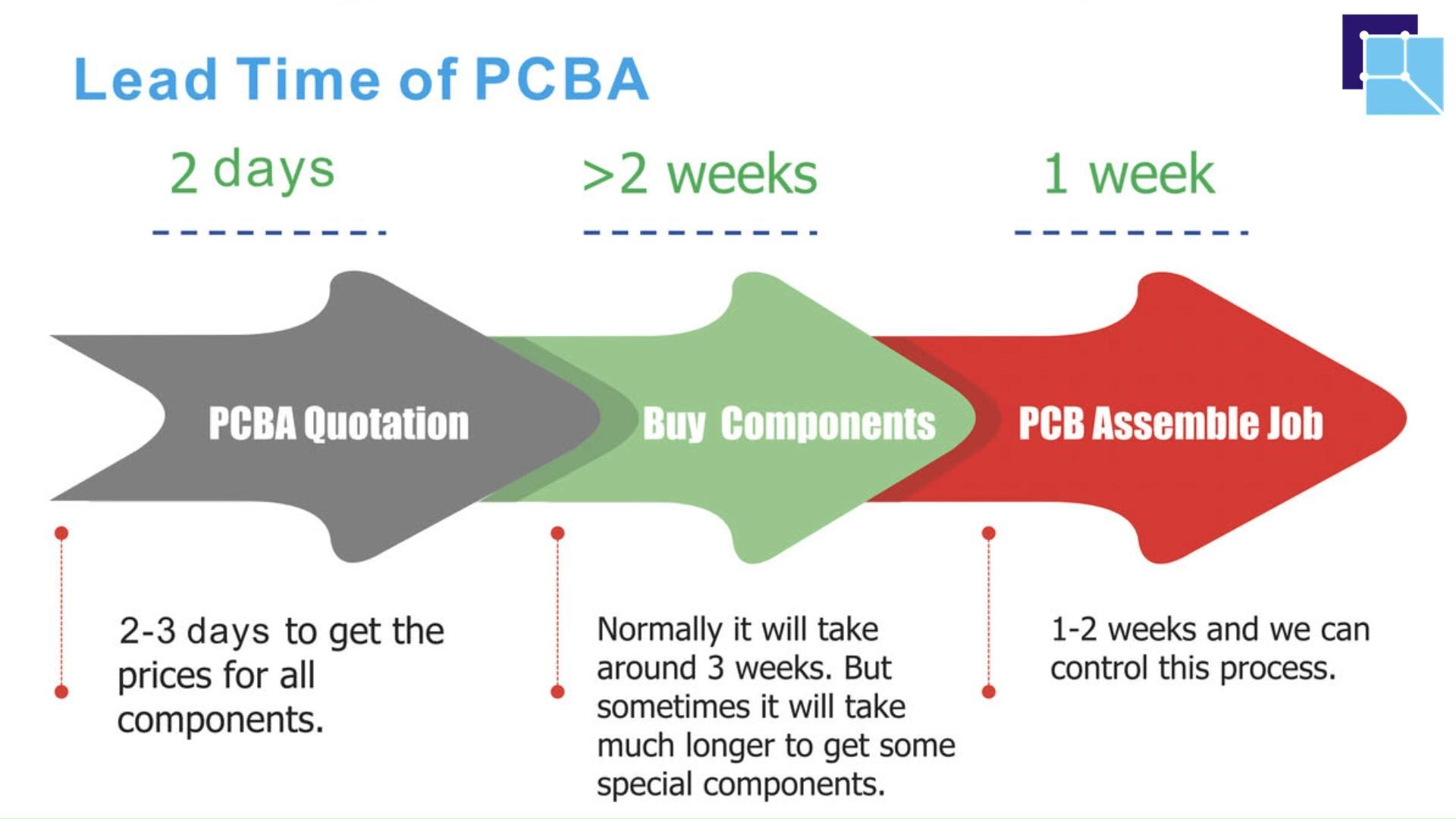
In PCBA manufacturing, soldering through-hole components (THT) remains a critical factor affecting efficiency and quality—issues like cold joints, bridging, and batch defects can skyrocket rework rates and delay deliveries. Wave Soldering technology is the ultimate solution, especially for PCB assemblies with through-hole components, as it directly determines product reliability, production efficiency, and market competitiveness.
Watch Our Wave Soldering Process in Action ? (Video: Full workflow from flux spraying to dual-wave soldering, with close-up solder joint inspection)
In this article, we’ll explore the importance of wave soldering and how our advanced equipment and strict process controls deliver high-precision, high-yield PCBA soldering services.
Unlike surface-mount technology (SMT), wave soldering specializes in through-hole components like connectors, electrolytic capacitors, and transformers. The molten solder "wave" ensures rapid, uniform soldering—ideal for high-volume production, with a single machine processing hundreds of PCBs per hour (50x faster than manual soldering).
For mixed-technology boards (SMT+THT), wave soldering precisely controls solder flow to prevent bridging or cold joints. Our dual-wave system (turbulent + smooth wave) ensures penetration into tight pin gaps while smoothing joint appearance, guaranteeing high-quality soldering for complex PCBs.
Poor soldering can cause signal interference, open circuits, or overheating. Our process adheres to IPC-A-610 standards, ensuring robust, conductive joints for automotive, industrial, and other high-reliability applications.
We use **fully automated dual-wave soldering machines with lead-free soldering (RoHS-compliant). Our dual-wave system reduces bridging by 30%, and optional nitrogen protection (<50ppm O₂) minimizes oxidation for shinier, stronger joints.
Every step—preheating → flux spraying → soldering → cooling—is monitored:
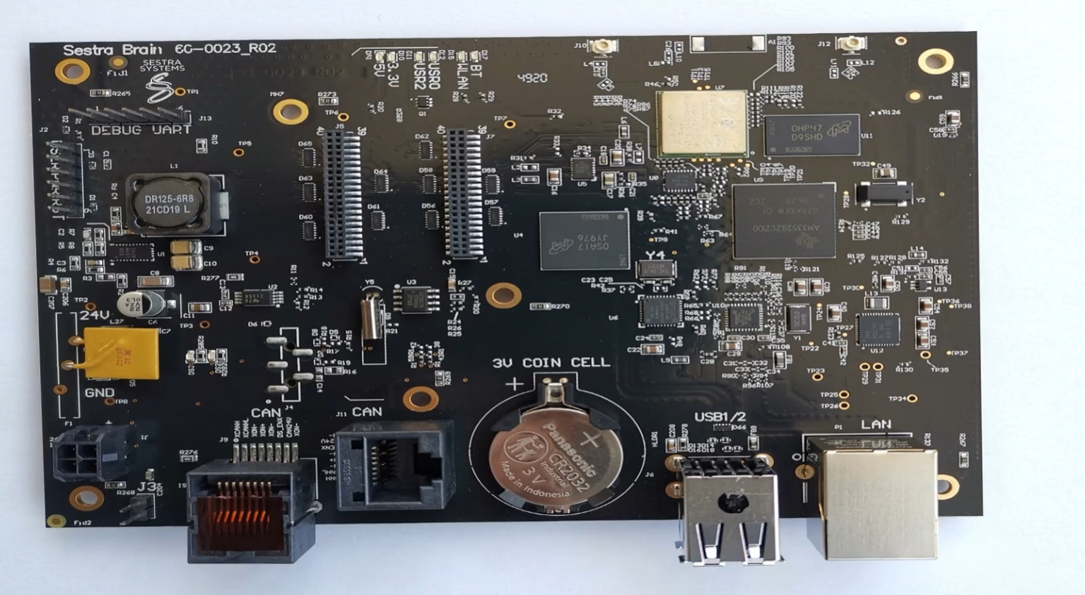
We handle thick-copper PCBs (3mm+), high-density boards (pin pitch ≤2.54mm), and heatsink-mounted PCBs, serving automotive (controllers, sensors), industrial (PLCs, inverters), and smart home (gateways) sectors with 500+ solved challenges.
From PCB fabrication → SMT assembly → testing, we streamline supply chains (no multi-vendor coordination), cutting time-to-market by 30%.
| Parameter | Original Setting | Optimized Setting | Impact |
|---|---|---|---|
| Preheat Temp | 120°C | 150°C (ramp-up) | Activates flux, reduces stress |
| Wave Height | 6mm | 8mm | Improves through-hole wetting |
| Conveyor Speed | 1.2m/min | 0.8m/min | Extends solder contact time |
| Our Edge | Industry Pain Points | Our Solution |
|---|---|---|
| ✅ High Yield | ❌ >3% defect rate | 99%+ soldering yield |
| ✅ Fast Prototyping | ❌ >7-day lead time for small batches | 48-hour trial production |
| ✅ Complex PCB Expertise | ❌ High-density soldering fails | 500+ proven cases |
| ✅ One-Stop PCBA | ❌ Managing 3+ suppliers | SMT + wave soldering + testing |
Need high-reliability, cost-effective wave soldering? Contact us today!
Upload your PCB files for a free DFM analysis + quote within 24 hours.
Free DFM review (identify soldering risks upfront).
20% off pilot batches (1–100 PCBs supported).
24/7 engineering support (1-on-1 process guidance).
Wave soldering is the cornerstone of reliable through-hole PCBA assembly. With cutting-edge equipment, rigorous controls, and deep expertise, we deliver high-yield, efficient soldering solutions. Let’s collaborate to boost your product’s competitiveness—request a custom quote now!
 Add: 803-804, Hisee International Commercial Center, Dongbin Road, Nanshan District, Shenzhen, China
 Tel: 0086-755-2664 8283
 E-mail: info@fully-hong.com


Copyright ©2025 Fully Hong Electronics Co.,Ltd. |A Professional And Reliable EMS/PCBA Partner.

 Previous